Quantcast
Channel: Cadence Digital Implementation Blogs
Viewing all 380 articles
Browse latest View live

Do you want to Flaunt your Expertise? Grab the Digital Badge Today!

$
0
0

When you achieve the credit for proficiency, do you want to show it to the world?

We know it isn’t easy to carry the actual physical badge (certificate) everywhere today. Why? Expenses, pandemic, making a list where to travel, to whom to show etc.

Don’t worry! We have an easy and cost-free solution for this. Become Cadence Certified with Digital Badges. How?

We have introduced courses for Digital Badge Exams for all the Cadence products for you!

Following is the list of courses in Genus and Joules product areas for which Digital Badge Exams are available:

  • Genus Synthesis Solution with Stylus Common UI
  • Advanced Synthesis with Genus Stylus Common UI
  • Low-Power Synthesis with Genus Stylus Common UI
  • Test Synthesis with Genus Stylus Common UI
  • Joules Power Calculator
  • Fundamentals of IEEE 1801 Low-Power Specification Format

And that’s not the end of the list! Find the complete list under this link or on our learning map – check for this icon . 

Upon passing the exam, you get a certificate from Cadence (verified by a third party, Credly). It can be shared on your LinkedIn profile, Facebook, Twitter, in your email signature, or wherever you like to show your competence (see example snapshot below).


The exams can be taken from Training Courses (cadence.com). Log in and search for the desired Badge Exam.

Find More Information: Check out the currently available certification courses and get information

Grab the Digital Badge today and flaunt it!


Power Is HOT and Touches Everything and Everybody! But the Challenge Is To Deal With Low Power During Design Synthesis; How?

$
0
0

Low-Power synthesis is one of the important stages in the full IC flow. Here, you synthesize the design from behavioral description to gates while optimizing for dynamic and leakage power using various techniques. We understand that it is not always easy to estimate power, but Cadence offers a solution in the form of a low-power synthesis flow with Genus.

Are you interested in exploring:

  • What the complete low-power synthesis flow is?
  • What the required inputs are?
  • How to configure power optimization?

There is a ONE-STOP solution to all these queries in the form of videos on "Setting and Running Power Optimization Flow in Genus Synthesis Solution," available on our Customer Support site (Cadence login required).

This channel contains videos that explore the basic low-power synthesis flow of the Genus Synthesis Solution. The videos cover the flow and steps to run the power optimization flow. The videos also explain the various commands and attributes used to run the power synthesis flow.

Video Title

Basic Low-Power Synthesis Flow in Genus Synthesis Solution Stylus CUI (Video) (cadence.com)

Related Resources

Enhance the Genus Synthesis experience with videos: Genus Synthesis Solution: Video Library

Do you want to Flaunt your Expertise? Grab the Digital Badge Today!

$
0
0

When you achieve the credit for proficiency, do you want to show it to the world?

We know it isn’t easy to carry the actual physical badge (certificate) everywhere today. Why? Expenses, pandemic, making a list where to travel, to whom to show etc.

Don’t worry! We have an easy and cost-free solution for this. Become Cadence Certified with Digital Badges. How?

We have introduced courses for Digital Badge Exams for all the Cadence products for you!

Following is the list of courses in Genus and Joules product areas for which Digital Badge Exams are available:

  • Genus Synthesis Solution with Stylus Common UI
  • Advanced Synthesis with Genus Stylus Common UI
  • Low-Power Synthesis with Genus Stylus Common UI
  • Test Synthesis with Genus Stylus Common UI
  • Joules Power Calculator
  • Fundamentals of IEEE 1801 Low-Power Specification Format

And that’s not the end of the list! Find the complete list under this link or on our learning map – check for this icon . 

Upon passing the exam, you get a certificate from Cadence (verified by a third party, Credly). It can be shared on your LinkedIn profile, Facebook, Twitter, in your email signature, or wherever you like to show your competence (see example snapshot below).


The exams can be taken from Training Courses (cadence.com). Log in and search for the desired Badge Exam.

Find More Information: Check out the currently available certification courses and get information

Grab the Digital Badge today and flaunt it!

Scan Mapping, Expectation Versus Reality? It's Time to Grab All the Scan Cells!

$
0
0

We all look for 100% perfection and want to turn our dreams (expectations) into reality as far as we can. Are you also looking for a magic wand to turn expectation into reality?

The story applies to DFT world too!! Design for Test (DFT) techniques comprehensively provide measures to test the manufactured device for quality and coverage. We expect 100% coverage and fault testing.

And the hard work for the design starts right from the beginning, but what if there is a glitch during the synthesis stage? You might encounter issues with the mapping of registers to scan flops during the synthesis stage. Does this mean you cannot reach the goal? Will you not be able to move forward further in the scan insertion process?

Well, we can't commit to the other things, but when it comes to the issue of mapping registers to scan cells, we can pitch in!!

Are you excited to explore the solution to ensure proper mapping of scan cells from the library?

There is a ONE-STOP solution for exploring the reasons for flops not mapped to the scan flops in the form of videos on "Why Are Sequential Elements Not Mapped to a Scan Flop?"; refer to the channel videos on https://support.cadence.com (Cadence login required).

This channel contains videos that explain why certain sequential cells are not mapped to the scan flops during scan insertion flow in Genus Synthesis Solution. The videos cover several scenarios and how to handle them.

Video Link:                                

Why Are Sequential Elements Not Mapped to a Scan Flop? (Video)  

Grab all the scan cells!!

Related Resources

Enhance the Genus Synthesis experience with videos: Genus Synthesis Solution: Video Library

For any questions, general feedback, or future blog topic suggestions, please leave a comment. 

Chris, Kris, Cris, Your Name, My Name; Does How You Spell the Name Matter to Conformal?

$
0
0

No matter how your name is spelt in different countries, and how they say it, once they get to know you, people identify you as the same person.

Ah! this is Chris, Cris, Kris, Kirshner, or Krishna. And I know this dude, even though he has transformed since I last saw him, and is 10 years older than what I remember. 

Likewise, different tools have different ways of naming the same design object and the default rules rarely match, but verification tools like Conformal must identify it as the same object; otherwise, comparison is difficult.

You can track those name changes, and during comparison identify those naming differences.

Conformal name-based mapping is the fastest mapping method. Take advantage of that, and use renaming rules to finish key point mapping.

This video shows how to apply renaming rules in Conformal Equivalence Checker.

Try the online course to get you started with Conformal Equivalence Checker - Conformal Equivalence Checking v21.1 (Online).

The course also has an associated exam to certify your knowledge of Conformal and display a badge on your Linkedin profile -  Conformal Equivalence Checking v21.1 (Badge Exam)

Related Training Bytes

Conformal Equivalence Checker – Mapping Issues (Video Channel)

What are Cut Points in Conformal LEC (Video)

Clock Gating Modeling in Conformal LEC (Video)

Related Blogs

Conformal Low Power Verification

Verifying Design Changes Does Not Have to be Difficult and Tedious — Make it Easier with Conformal Equivalence Checker

Voltus Voice: Overcoming Design Challenges Using Voltus Documentation—The Definitive Training Video

$
0
0
This post facilitates easy access to the Voltus Help and Documentation through the most useful resources from the Cadence support and corporate websites directly from the tool interface.(read more)

Training Insights - Achieving a Holistic Power-Aware Design by Getting Low-Power Right

$
0
0
This blog post mentions the Cadence Low Power Solution, a design-to-signoff methodology, that helps you implement several low-power techniques to reduce both dynamic and leakage power during synthesis and design implementation. Formal verification can be run to ensure the functionality of a low-power design.(read more)

What's Behind the 5% Die-Area Shrink and 12% Power Saving by MediaTek?

$
0
0

Leveraging Cadence Cerberus AI-Enabled Chip Optimization Solution MediaTek Achieves Transformative PPA and Improved Productivity

The semiconductor industry is in the midst of a global renaissance. With the advent of technologies like 5G, autonomous driving, hyperscale compute, and the Internet of things, there has been an explosion in demand for electronics. Consumers want chips that must have more functionality, more compute, and faster data transmission speed. But these complex chips must also be produced faster to keep up with the increasing demand.

So, to stay ahead of the competition and meet the increasing demand, design companies must produce chips with better PPA and find new ways to improve productivity. This has been made possible by an AI-enabled chip optimization solution – Cadence Cerebrus.

This Intelligent Design Explorer is a transformational ML-based technology with a unique reinforcement learning engine, which optimizes the chip design options to deliver improved PPA beyond human potential with significantly less engineering effort and overall time to tapeout.

The proof is in the pudding. In the recent CadenceLIVE Silicon Valley 2022, Tony Han, Director of MediaTek, spoke about leveraging Cadence Cerebrus solution in their design flow, enabling them to shrink the die size by 5% and lowering total power by more than 12% on a critical macro. Using Machine Learning Model also reduced overall optimization time from 18 days to 8.3days, significantly improving engineering productivity.

"At MediaTek, we are resolute in delivering optimal PPA, making the Cadence Cerebrus AI-based solution the most logical choice for our latest, advanced-node projects," - Harrison Hsieh, MediaTek.

Key Cerebrus Features that Led MediaTek to Deploy Cerebrus in Production flow 

After integrating Cadence Cerebrus, MediaTek observed a considerable PPA boost, productivity improvements, and smaller die by enabling the Cerebrus Floorplan Optimization App.

Improved Total Power 

While moving from baseline flow to Cerebrus optimized flow on a critical macro, MediaTek observed 26.3% improved Total Negative Slack and 9.6% improved Total Power. After instantiating this macro inside an IP, the Fmax was improved by 150MHz, along with a 12.5% reduction in Total Power.

Phenomenal Productivity improvement

Once Cadence Cerebrus is run on Early RTL, it generates a Machine Learning Model, which can then be reused by the newer release of the same RTL or similar designs to transfer the intelligence captured from the previous run. This helps the engineering teams to reduce overall optimization cycle time and use compute resources efficiently. MediaTek made use of this feature, helping them reduce the design time from 18days down to 8.3 days, improving run time productivity by 53.88% 

Floorplan Optimization Cerebrus App

MediaTek used the Floorplan Optimization Cerebrus App to optimize the die size. With the increasing complexity of designs, it's impossible to manually optimize the macro placement, die size, core shape, and other aspects of the floorplan. Using ML-based optimization, Cerebrus can explore the most optimal solution space, which otherwise would not have been possible.                                                 

Ease of Integration: Cadence Cerebrus Adoption into MediaTek Production Flow

Cadence Cerebrus is easy to adopt because it easily wraps around any custom flow without requiring a significant overhaul of the current chip design flow. As a result, it was easy for MediaTek to port their existing full flow using Genus, Innovus, and Tempus into the Cerebrus environment for production use. This methodology also keeps the baseline flow intact, allowing comparisons of various metrics generated during multiple iterations.

Conclusion

Cadence Cerebrus Optimization Solution helped MediaTek achieve better PPA and Productivity. They saw a reduction of 12.5% in Total Power on a critical macro, a die size reduction of 5%, and productivity improvement of over 53%. All this and ease of adoption led them to deploy Cerebrus for production use on a wide scale across the company.

Learn More


Voltus Voice: Playback 2021 - Power Integrity Blogs At a Glance

$
0
0
A recap of the power integrity posts in the Voltus Voice blog series through 2021. (read more)

RTL-to-GDSII Flow: I Am Not a Tool but Can Help You Implement Your Entire Design!

$
0
0

Passion motivates and helps you pursue it further, but gaining expertise requires time and effort. For example, photography is a popular hobby because anyone can take a picture. But to gain expertise requires time and effort to experiment with various techniques to improve your skills.                                                                                                                                                                                                                                                                      


Likewise, given an innovative design idea, it takes an efficient methodology and implementation flow to generate it to a GDSII. To achieve this, we use RTL-to-GDSII flow, also known as Digital flow or ASIC flow, which includes many stages in designing an IC in the semiconductor industry. Starting from RTL coding, simulating the RTL, synthesizing and testing, implementing the logic as a physical layout, and finally generating a GDSII file after timing signoff, each stage in the flow has unique techniques and complexities. 

Don’t get overwhelmed with terminology. Get hooked on the world of Cadence_RTL-to-GDSII_Flow 4_0 and start exploring the ABCs of the design flow process.

This course teaches how to implement a design idea from RTL-to-GDSII flow using Cadence® tools. You will learn how to deal with these challenges while running the flow, such as resolving errors in the log file, debugging the timing violations, and fixing setup and hold violations. After completing the lecture, you can download a lab database and manual to test your knowledge at every stage.

After completing this course, you will be able to:

  • Code a design in Verilog as per the design specification provided
  • Compile, elaborate, and simulate your design
  • Synthesize your design
  • Design for test
  • Run equivalency checking at different stages of the flow
  • Floorplan a design
  • Run placement, optimization, clock tree synthesis, and routing on your design
  • Run signoff checks to ensure that can able to fabricate a chip.
  • Write out a GDSII file.


Steps to follow to get enrolled in this course:

  1. Log on to support.cadence.com with your registered Cadence ID and password.
  2. Select Learning from the menu > click Online Courses.
  3. Search for Cadence_RTL-to-GDSII_Flow 4_0 using the search bar.
  4. Select the course and click the Enroll button.


Digital Badge Available

The course also has an associated exam to certify your knowledge of RTL-to-GDSII flow and display a digital badge on your Linkedin profile – Cadence RTL-to-GDSII v4.0 (Badge Exam)


 Related Resources

Online courses

Blogs

Training Bytes

 For more information on Cadence’s digital design and signoff products and services, visit www.cadence.com.

Happy learning! Thank You.

What's Behind the 5% Die-Area Shrink and 12% Power Saving by MediaTek?

$
0
0

Leveraging Cadence Cerberus AI-Enabled Chip Optimization Solution MediaTek Achieves Transformative PPA and Improved Productivity

The semiconductor industry is in the midst of a global renaissance. With the advent of technologies like 5G, autonomous driving, hyperscale compute, and the Internet of things, there has been an explosion in demand for electronics. Consumers want chips that must have more functionality, more compute, and faster data transmission speed. But these complex chips must also be produced faster to keep up with the increasing demand.

So, to stay ahead of the competition and meet the increasing demand, design companies must produce chips with better PPA and find new ways to improve productivity. This has been made possible by an AI-enabled chip optimization solution – Cadence Cerebrus.

This Intelligent Design Explorer is a transformational ML-based technology with a unique reinforcement learning engine, which optimizes the chip design options to deliver improved PPA beyond human potential with significantly less engineering effort and overall time to tapeout.

The proof is in the pudding. In the recent CadenceLIVE Silicon Valley 2022, Tony Han, Director of MediaTek, spoke about leveraging Cadence Cerebrus solution in their design flow, enabling them to shrink the die size by 5% and lowering total power by more than 12% on a critical macro. Using Machine Learning Model also reduced overall optimization time from 18 days to 8.3days, significantly improving engineering productivity.

"At MediaTek, we are resolute in delivering optimal PPA, making the Cadence Cerebrus AI-based solution the most logical choice for our latest, advanced-node projects," - Harrison Hsieh, MediaTek

Key Cerebrus Features that Led MediaTek to Deploy Cerebrus in Production flow 

After integrating Cadence Cerebrus, MediaTek observed a considerable PPA boost, productivity improvements, and smaller die by enabling the Cerebrus Floorplan Optimization App.

Improved Total Power 

While moving from baseline flow to Cerebrus optimized flow on a critical macro, MediaTek observed 26.3% improved Total Negative Slack and 9.6% improved Total Power. After instantiating this macro inside an IP, the Fmax was improved by 150MHz, along with a 12.5% reduction in Total Power.

Phenomenal Productivity improvement

Once Cadence Cerebrus is run on Early RTL, it generates a Machine Learning Model, which can then be reused by the newer release of the same RTL or similar designs to transfer the intelligence captured from the previous run. This helps the engineering teams to reduce overall optimization cycle time and use compute resources efficiently. MediaTek made use of this feature, helping them reduce the design time from 18days down to 8.3 days, improving run time productivity by 53.88% 

Floorplan Optimization Cerebrus App

MediaTek used the Floorplan Optimization Cerebrus App to optimize the die size. With the increasing complexity of designs, it's impossible to manually optimize the macro placement, die size, core shape, and other aspects of the floorplan. Using ML-based optimization, Cerebrus can explore the most optimal solution space, which otherwise would not have been possible. They achieved up to 6% improvement.                                   

Ease of Integration: Cadence Cerebrus Adoption into MediaTek Production Flow

Cadence Cerebrus is easy to adopt because it easily wraps around any custom flow without requiring a significant overhaul of the current chip design flow. As a result, it was easy for MediaTek to port their existing full flow using Genus, Innovus, and Tempus into the Cerebrus environment for production use. This methodology also keeps the baseline flow intact, allowing comparisons of various metrics generated during multiple iterations.

Conclusion

Cadence Cerebrus Optimization Solution helped MediaTek achieve better PPA and Productivity. They saw a reduction of 12.5% in Total Power on a critical macro, a die size reduction of 5%, and productivity improvement of over 53%. All this and ease of adoption led them to deploy Cerebrus for production use on a wide scale across the company.

Learn More

Brain on Fire - AI/ML Art Creation

$
0
0

No matter how you feel about the topic, we're definitely past the turning point in history where most humans interact with machines much more than other humans.

Advancements in artificial intelligence and machine learning (AI/ML) have helped us develop immensely useful and sometimes just-for-fun applications including image creations with AI inputs.

Look at these images generated from text for example, with some weights and presets:

Creation Settings
Preset Style - 
MatteText Prompts - "Brain on fire" Weight: 1, "just head" Weight: 1, "no body" Weight: 1; Runtime - Short.

       Brain on fire 1 

Creation Settings
Preset Style - Cosmic, Text Prompts - "Brain on fire" Weight: 1, "cosmic illustration" Weight: 0.9, Runtime - Short.

Brain on fire 2

The images generated can be stunning or sadly disappointing depending on the user's perspective and imagination; meaning it is subjective. Nonetheless, you will tend to agree that the nature of this AI is such that your inputs and weights assigned gives you reasonably approximate outcomes of what you might expect in a reasonable amount of time. Given the chance at multiple tries and specifying different weights, you might find yourself the creator of a masterpiece coveted by many. 

Cadence tools such as Innovus Implementation use AI to improve your turnaround time (TAT) in various forms.

Cadence Cerebrus Intelligent Chip Explorer is a revolutionary, machine learning-driven, automated approach to chip design flow optimization.

Rather than specific tool inputs, Cadence Cerebrus uses weights, similar to our AI-generated art pieces, to optimize your flow from RTL to GDS, while optimizing your design for power, performance, and area, and in the process generate machine learning (ML) models for the type of design and tools you choose. 

These optimized Cadence Cerebrus machine learning models can become the perfect preset styles for your future design projects. 

To learn more, go to http://support.cadence.com and look for Cadence Cerebrus, or sign up for the class. 

Voltus Voice: Five Great Features to Enhance Your Full-Chip Power Signoff

$
0
0
This blog shares five great features to unlock the potential of your digital designs and enhance full-chip power signoff.(read more)

Training Insights – Design Robustness Analysis Application: Aging-Aware STA

$
0
0
This blog post describes the phenomenon of Aging, the factors affecting it, and how Cadence solves this problem with its groundbreaking Aging-Aware STA technology enabled using Liberate, Spectre, and Tempus STA.(read more)

SSV 22.1 Base Release Now Available

$
0
0
The Silicon Signoff and Verification (SSV) 22.1 release is now available for download.(read more)

Resolve Congestion and Physical Design Challenges Using Cadence Support and RAKs

$
0
0

Physical design challenges such as congestion, routing, on-chip variation (OCV), and unconstrained paths are significant issues in achieving the design goals. Managing the routing congestion and physical design challenges with the least amount of effort is a big problem for physical design engineers. Further, the usage of advanced nodes and increasing functionality over SoC is leading to rising complexity and conflicting PPA and TAT goals. 

Cadence support and rapid adoption kits (RAKs) enable our partners to achieve the best results and resolve such challenges quickly with the least effort. All such efficient practices with advanced solutions to handle the physical design challenges are available at the Cadence Support portal site. It has collated years of experience with experts to supply tips and techniques to help meet your design PPA and TAT requirements. This resource is available 24X7.

This blog talks about mitigating these physical design challenges using Cadence support.

How to Mitigate Congestion/Routing Congestion?

With the adoption of advanced nodes and industry inclination towards reducing metal layers available for routing, congestion is increasing and is a bottleneck in meeting PPA and TAT goals. Analyzing congestion at an early stage will aid in a quicker design closure even though it appears at the routing stage of the design.

Congestion may result due to:

  • Bad coding practices (Using System C)
  • Pipelined architectures and shared
  • Shared registers

It is very important to consider the congestion, which can be reduced using the options below:

  • Correctly following process node/design mode settings
  • Set PlaceMode settings
  • Congestion Maps/ density screens
  • Cell padding etc.
  • Using track opt-based routing

Track opt-based routing makes faster design closure possible, which reduces the duration gap between pre-route and post-route. You may find more details and recommendations for resolving the congestion in the RAK.

What is Clock Tree Synthesis (CTS)?

As digital design challenges grow with each process node shrinking, new placement, routing, and clocking capabilities are needed to meet PPA and TAT goals. One of the main CTS goals is to achieve minimum clock tree area/power. 


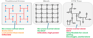
 Physical Design Challenges- Clock Tree SynthesisAlthough the schemes such as mesh and conventional H-tree result in a higher quality of results (QoR) than normal CTS, they suffer from a low degree of freedom in a clock tree design, man-hours for creation, and high-power consumption. Traditional schemes that use skew slack, minimization, and performing CTS suffer from a timing gap between ideal pre-CTS and propagated clocks post-CTS. Please refer to clock tree synthesis debugging techniques to learn more about CTS.
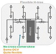
Finding the ideal balance between avoiding blockages and power rails, Cadence Flex-H Tree to improve PPA

adhering to partition, module, and power domain limits, and optimizing insertion delay, power, and skew is made easier with the help of Cadence, flexible - H. 

The integration of CTS and physical optimization is made possible by clock concurrent optimization (CCOpt). The Early Global Route (eGR), which also delivers further improvements in total negative slack (TNS) and worst negative slack (WNS), as well as predictable design closure, is a feature of the Innovus Implementation system. CCOpt with Innovus offers the below advantages with an excellent CTS:

 Cadence Innovus - improve PPA

  • Fixes signal integrity issues before detail route
  • Reduces the time gap between pre-route and post-route
  • Allows change in netlist and cell locations

What is Statistical On-chip variation (SOCV) Debugging RAK?

The nominal delays of all instances have traditionally been scaled with a single derating factor, in OCV, to simulate the on-chip process variation. This may result in over-optimism or pessimism, excessive design, and a longer turnaround time for timing closure. The logic timing is impacted by the timing changes caused by (OCV). These variances could cause ICs from one batch of wafers to perform "quick" or "slow" in comparison to nominal estimates. If a design successfully completes both the slow corner and fast corner timing analyses, it is said to have complied with the time constraints. By addressing these obstacles, statistical OCV (SOCV) offers a fair balance between run time and accuracy for modeling variance. For each instance in the design, SOCV calculates the effect of local process variations on the delay and slew at a specific global variation corner. RAK SOCV debugging offers several ways to fix problems and debug on-chip variation. The SOCV debugging RAK provides various solutions to issues and debugging on-chip variation (OCV). It helps in faster debugging of SOCV-related issues, including investigating various timing analysis problems, reporting SOCV timing results, performing SOCV timing calculations, etc.

What's there in Unconstrained Path Debugging RAK?

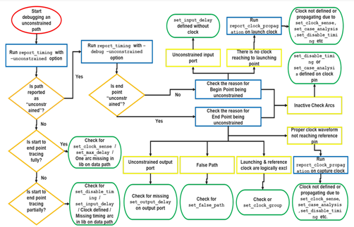
During static timing analysis (STA), designers often come across timing paths that are not analyzed by the STA tool. These paths can be intended to be analyzed, but due to constraint, setup, library, etc., issues may result in the path not being reported as a constraint timing path. All paths and ports should be constrained for ideal placements and the finest-suited outcomes. The uncontrolled paths that arise from setup, library, setup constraints, and other factors make it difficult to achieve the best placement and routing outcomes. Unconstrained path debugging RAK includes a thorough manual and a lab that goes over a variety of scenarios in which a path won't be reported as a constrained path. This article also includes a flowchart that illustrates the debugging strategy to be used based on the observations made at each stage to determine why the path isn't reported as a limited path.

When it comes to meeting timing constraints, Cadence's Tempus solution takes on the most complex problems, including complete signal integrity and others. It provides a solution to the unjustified pessimism brought on by on-chip fluctuation. It is capable of handling the ultra-low voltage effects at 7nm and below, which leads to statistical variance.

Conclusion

Cadence assistance and RAKs make use of the finest plans to overcome the physical design challenges and assist partners in achieving design objectives with less time and effort. The early analysis would permit a quicker design closure. Different flow adjustments made by designers aid in design convergence while achieving PPA objectives. Different flow adjustments aid in design convergence while achieving PPA objectives. More users utilize SOCV analysis as we advance to smaller geometry nodes to combat pessimism. The SOCV debugging RAK offers users a range of SOCV-related issues, fixes, and debugging techniques.

Learn More

Relax in Summer with Cooler IC chips and Ice-Cream! Do you want to Explore the Recipe?

$
0
0

Are you passionate about cooking? Err... Don't think it is a regular cooking class.

Here we tend to cook cooler power solutions! 

Do you know creating a cooler IC chip is as easy as enjoying the ice-cream in summer to beat the heat? 

Low-Power synthesis is one of the important stages in the full IC flow. Using various techniques, you synthesize the design from behavioral description to gates while optimizing for dynamic and leakage power.

Well, the ingredients for the recipe could vary based on your design and specifications.

Is it a regular low-power flow?

Are you using multiple supply voltage (MSV) design, power shutoff (PSO) synthesis, and dynamic voltage frequency scaling (DVFS) synthesis techniques in the form of the IEEE 1801 power intent file?


 In this cooking session, you will be:

  • Identifying power reduction techniques
  • Setting up and running low-power synthesis flow
  • Enabling clock gating
  • Annotating switching activity and running RTL power estimation
  • Running optimizations to reduce dynamic and leakage power consumption
  • Analyzing power results
  • Using IEEE 1801 for designs with MSV and PSO methodology
  • Troubleshooting low-power design
  • Identifying low-power design checks using Cadence®Conformal® software
  • Identifying and debugging design scenarios in IEEE 1801
  • Identifying Genus-JoulesIntegration 

 We understand that it is not always easy to estimate power, but we can guide you!

There is a ONE-STOP session to all these requirements in the form of the training course on "Genus Low-Power Synthesis Flow with IEEE 1801 v21.1 (Online)".

Course Title: Genus Low-Power Synthesis Flow with IEEE 1801


Related Resources

Enhance the Genus Synthesis experience with videos: Genus Synthesis Solution: Video Library

Voltus Voice: How to Find Functional Power Vectors that Matter Quickly

$
0
0
Vector profiling enables ASIC designers to quickly identify areas with maximum activity and power consumption when analyzing long simulation vectors, accelerating power signoff of billion-node designs. Focusing on meaningful events reduce the power signoff analysis runtime and memory usage drastically, having a direct impact on time-to-market. Check out this blog to know more. (read more)

HLS for AI/ML Models: TensorFlow to RTL

$
0
0
Artificial Intelligence (AI) plays a key role in semiconductors to meet the challenging demand and rising customer expectations. But implementing these AI models in Hardware (FPGA) is challenging. AI developers generally use TensorFlow/Caffe model, w...(read more)

Training Insights – Webinar – Transforming your Timing Signoff Experience with Tempus SSV221: Registrations Open

$
0
0
This webinar encourages you to learn and apply the latest innovations in the Cadence®︎ Tempus Timing Solution SSV221 Release.(read more)
Viewing all 380 articles
Browse latest View live